Monday, March 23, 2015

SPI Host Controller and Device Programming

This page describes how to write a program to drive SPI host controller to communicate a SPI device (e.g., flash part) via SPI protocol. We know SPI has 4 wires, and SPI host controller has 2 FIFO, RX FIFO and TX FIFO. How does host controller work with both FIFOs and 4 wires SPI. I consider the Read-Id (EFh) command of the flash part W25Q80DV is an simplest example to describe the mechanism.

Please refer my previous page to understand Data Transmission via SPI.

The following block diagram uses a simple model to describe the hardware mechanism of SPI Host Controller with RX/TX FIFO, registers accessed by a program, and 4 SPI wires connected to a SPI device. This diagram skips the shift register in SPI Host Controller. It also skips the details hardware components of the SPI device.


SPI 4 Wires.

SPI has 4 wires, CS, CLK, MOSI, and MISO. Please refer the wiki page, SPI Bus.

Two FIFOs.

TX FIFO transmits data to a SPI device (e.g., flash part) via MOSI. When data are transmitted, CLK is also enabled. Therefore RX FIFO might receive dummy data via MISO at the same time.

Registers of SPI Host Controller

CS register selects a SPI device to begin to communicate via SPI.

Data register is a window to write data into TX FIFO and read data from RX FIFO.

TXL (TX Level) register reports the number of elements in TX FIFO.

RXL (RX Level) register reports the number of elements in RX FIFO.

SPI Programming.

The routine SpiTransfer() transmits Request with RequestSize bytes to a SPI device and receives Response with ResponseSize bytes from the SPI device.

SpiTransfer (
  IN UINT8 *Request
  IN UINTN RequestSize
  OUT UINT8 *Response
  IN UINTN ResponseSize
  )
{
  Dev = GetHcDevice ();

  // Select a SPI device.

  Dev->Hc->CsReg = 0;

  // Transmit the request to the SPI device via MOSI.

  for (i = 0; i < RequestSize; i++) {
    Dev->Hc->DataReg = Request [i]; // put a byte in TX FIFO.
    Delay (...); // wait for transmitting the byte.
    Dummy = Dev->Hc->DataReg; // clean a received dummy in RX FIFO.
  }

  // Clean dummy data in RX FIFO.

  while (Dev->Hc->RxlReg) { // if RX FIFO has dummy data,
    Dummy = Dev->Hc->DataReg; // clean the received dummy in RX FIFO.
  }

  // Receive a response from the SPI device via MISO.

  for (i = 0; i < ResponseSize; i++) {

    // put a dummy in TX FIFO to trigger CLK so that RX FIFO 
    // will receive data from the SPI device via MISO.
    Dev->Hc->DataReg = Dummy;     

    Delay (...); // wait for the dummy is transmitted. 
    Response [i] = Dev->Hc->DataReg; // Receive data in RX FIFO.
  }

  // Free the SPI device.

  Dev->HC->CsReg = 1;

}

-Count


Sunday, March 22, 2015

Data Transmission via SPI

As we know that SPI has 4 wires to transmit and receive data between a mast and a slave. Please refer the wiki page, SPI Bus for the detail information first.

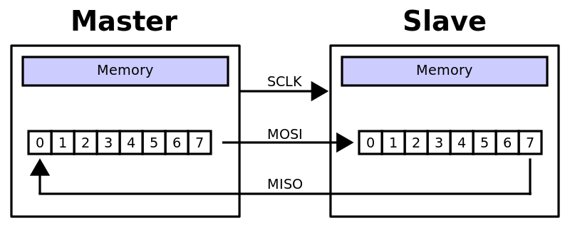
The information is not enough for us to write a SPI program to drive a master device to transmit/receive data to/from a slave device. I'm interested the below picture of the SPI Bus wiki page because it can help us for writing the program.


We can imagine that there is a ring composed of MOSI, MISO, and two shift registers. A basic communication program is to send a request and to wait for a response. For SPI, we send a request to a slave via MOSI and wait for a response from a slave via MISO.

Read-Id Command of Flash Part

The read-id command of the flash part, W25Q80DV is an example because I consider it is the simplest command for programming.


We want to write a program to get flash part id. The program transmit 9F to the flash part via MOSI and receive EF-40-14 from the flash part via MISO.

MOSI: 9F // Transmit Read ID command (9F) to get ID information
MISO: EF, 40, 14 // Receive ID information.

How do we  write the program?

Transmit Data

Because SPI is a ring, when the master transmits a command with 1 byte (e.g., 9F) to the slave (flash part), the master also receives a dummy 1 byte from slave. The command is stored in TX FIFO and the dummy 1 byte is stored in RX FIFO. Therefore when the master transmits the command, it must clear dummy bytes in RX FIFO.

Receive Data

Please remember that SPI is a ring. If the master wants to receive data (e.g., id information with 3 bytes) from the slave (e.g., flash part), the master must send dummy data (e.g., 3 zero bytes) to push the slave to response data (e.g., EF-40-14.)

TX FIFO and RX FIFO

The master usually has 2 FIFOs. TX FIFO is to transmit data to the shift register and RX FIFO is to receive data from the shift register. I'll have another page SPI Host Controller and SPI Device Programming to describe the topic.

-Count